- Tel: 86-755-23941515
- Email: Sales@xida-electronics.com
The LF356-MIL device are the first monolithic JFET input operational amplifiers to incorporate wellmatched, high-voltage JFETs on the same chip with standard bipolar transistors (BI-FET™ Technology). These amplifiers feature low input bias and offset currents/low offset voltage and offset voltage drift, coupled with offset adjust, which does not degrade drift or common-mode rejection. The devices are also designed for high slew rate, wide bandwidth, extremely fast settling time, low voltage and current noise and a low 1/f noise corner.
 Figure: LF356 PCB Symbol

Figure: LF356 Footprint

Figure: LF356 3D Models
 Figure: LF356 Pin Configuration
 Figure: LF356 Simplified Schematic
 Figure: LF356 Block Diagram
– Replace Expensive Hybrid and Module FET Op Amps
– Rugged JFETs Allow Blow-Out Free Handling Compared With MOSFET Input Devices
– Excellent for Low Noise Applications Using Either High or Low Source Impedance—Very Low 1/f Corner
– Offset Adjust Does Not Degrade Drift or Common-Mode Rejection as in Most Monolithic Amplifiers
– New Output Stage Allows Use of Large Capacitive Loads (5,000 pF) Without Stability Problems
– Internal Compensation and Large Differential Input Voltage Capability
– Low Input Bias Current: 30 pA
– Low Input Offset Current: 3 pA
– High Input Impedance: 1012 Ω – Low Input Noise Current: 0.01 pA/√Hz
– High Common-Mode Rejection Ratio: 100 dB
– Large DC Voltage Gain: 106 dB
– Extremely Fast Settling Time to 0.01%: 1.5 μs – Fast Slew Rate: 12 V/µs – Wide Gain Bandwidth: 5 MHz
– Low Input Noise Voltage: 12 nV/√Hz
You can download the datasheet from the link given below:
| Product Attribute | Attribute Value |
| Manufacturer: | Texas Instruments |
| Product Category: | Operational Amplifiers - Op Amps |
| RoHS: | Details |
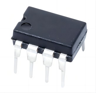
| Mounting Style: | Through Hole |
| Package / Case: | PDIP-8 |
| Number of Channels: | 1 Channel |
| Supply Voltage - Max: | 44 V |
| GBP - Gain Bandwidth Product: | 5 MHz |
| Output Current per Channel: | 25 mA |
| SR - Slew Rate: | 12 V/us |
| Vos - Input Offset Voltage: | 2 mV |
| Supply Voltage - Min: | 10 V |
| Minimum Operating Temperature: | 0℃ |
| Maximum Operating Temperature: | + 70℃ |
| Ib - Input Bias Current: | 200 pA |
| Operating Supply Current: | 5 mA |
| Shutdown: | No Shutdown |
| CMRR - Common Mode Rejection Ratio: | 100 dB |
| en - Input Voltage Noise Density: | 12 nV/sqrt Hz |
| Series: | LF356 |
| Packaging: | Tube |
| Brand: | Texas Instruments |
| Height: | 3.3 mm |
| In - Input Noise Current Density: | 0.01 pA/sqrt Hz |
| Input Type: | Rail-to-Rail |
| Length: | 9.27 mm |
| Maximum Dual Supply Voltage: | +/- 18 V |
| Minimum Dual Supply Voltage: | +/- 5 V |
| Operating Supply Voltage: | 10 V to 36 V, +/- 5 V to +/- 18 V |
| Pd - Power Dissipation: | 670 mW |
| Product: | Operational Amplifiers |
| Product Type: | Op Amps - Operational Amplifiers |
| PSRR - Power Supply Rejection Ratio: | 80 dB |
| Subcategory: | Amplifier ICs |
| Supply Type: | Dual |
| Technology: | BiFET |
| Vcm - Common Mode Voltage: | 10 V to 36 V |
| Voltage Gain dB: | 106.02 dB |
| Width: | 6.35 mm |
| Unit Weight: | 588.100 mg |
Texas Instruments Incorporated (TI) is an American technology company headquartered in Dallas, Texas, that designs and manufactures semiconductors and various integrated circuits, which it sells to electronics designers and manufacturers globally. It is one of the top 10 semiconductor companies worldwide based on sales volume.The company's focus is on developing analog chips and embedded processors, which account for more than 80% of its revenue. TI also produces TI digital light processing technology and education technology products including calculators, microcontrollers and multi-core processors. The company holds 45,000 patents worldwide as of 2016.
Note: Please check their parameters and pin configuration before replacing them in your circuit.
An operational amplifier has two input pins and one output pin. Its basic role is to amplify and output the voltage difference between the two input pins.
Op-Amp (operational amplifier)
Originally, op-amps were so named because they were used to model the basic mathematical operations of addition, subtraction, integration, differentiation, etc. in electronic analog computers. In this sense a true operational amplifier is an ideal circuit element.
Op amps are composed of standard components such as—notice—transistors, resistors, diodes, and so forth, and a capacitor right here. The input terminals of an op amp are connected to the bases of transistors.
These are abbreviated as Op-Amps. It is capable of performing basic mathematical operations that is addition, subtraction, multiplication, and division. The single output terminal is capable of sinking and sourcing both the current and the voltage signals.
Op amps need high input impedance because they are voltage-gain devices. In order for voltage to drop across the input, the impedance has to be very high, as ohm's law states, V=IR. It's also important to prevent the loading effect. If the impedance were small, the current draw would be high.

 0
0