- Tel: 86-755-23941515
- Email: Sales@xida-electronics.com
The KSZ9031RNX is a completely integrated triple-speed (10BASE-T/100BASE-TX/1000BASE-T) Ethernet physicallayer transceiver for transmission and reception of data on standard CAT-5 unshielded twisted pair (UTP) cable. The KSZ9031RNX provides the Reduced Gigabit Media Independent Interface (RGMII) for direct connection to RGMII MACs in Gigabit Ethernet processors and switches for data transfer at 10/100/1000 Mbps.
This blog will introduce KSZ9031RNXIC-TR systematically from its features, pinout to its specifications, applications, also including KSZ9031RNXIC-TR datasheet and so much more.
The following figure is the diagram of KSZ9031RNXIC-TR pinout.

KSZ9031RNXIC-TR Pinout
The followings are KSZ9031RNXIC-TR Symbol, Footprint, and 3D Model.

KSZ9031RNXIC-TR Symbol

KSZ9031RNXIC-TR Footprint

KSZ9031RNXIC-TR 3D Model
The following figure shows the block diagram of KSZ9031RNXIC-TR.

KSZ9031RNXIC-TR Block Diagram
A crystal or external clock source, such as an oscillator, is used to provide the reference clock for the KSZ9031RNX. The reference clock is 25 MHz for all operating modes of the KSZ9031RNX.
The KSZ9031RNX uses the AVDDH supply, analog 3.3V (or analog 2.5V option for commercial temperature only), for the crystal/clock pins (XI, XO). If the 25 MHz reference clock is provided externally, the XI input pin should have a minimum clock voltage peak-to-peak (VPP) swing of 2.5V reference to ground. If VPP is less than 2.5V, series capacitive coupling is recommended. With capacitive coupling, the VPP swing can be down to 1.5V. Maximum VPP swing is 3.3V +5%.
The following figure shows the reference clock connection to XI and XO of the KSZ9031RNX.

KSZ9031RNXIC-TR Circuit Diagram
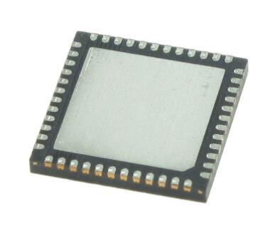
The following diagram shows the KSZ9031RNXIC-TR package.


 0
0